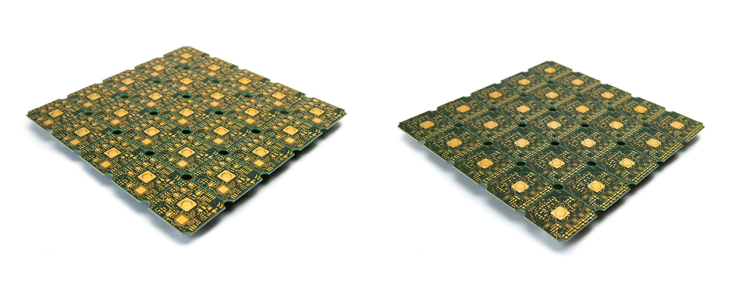
Metal Inlay Technology - Metal Inlay PCB
Optimal Heat Dissipation Concept via Embedded Inlays
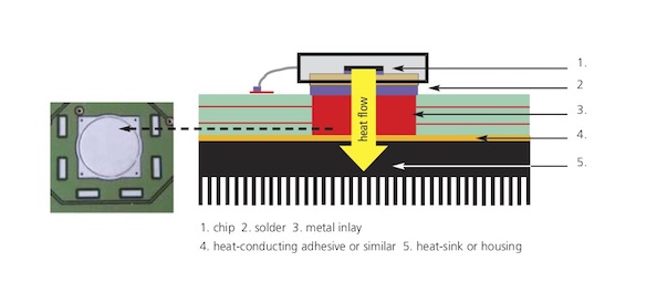
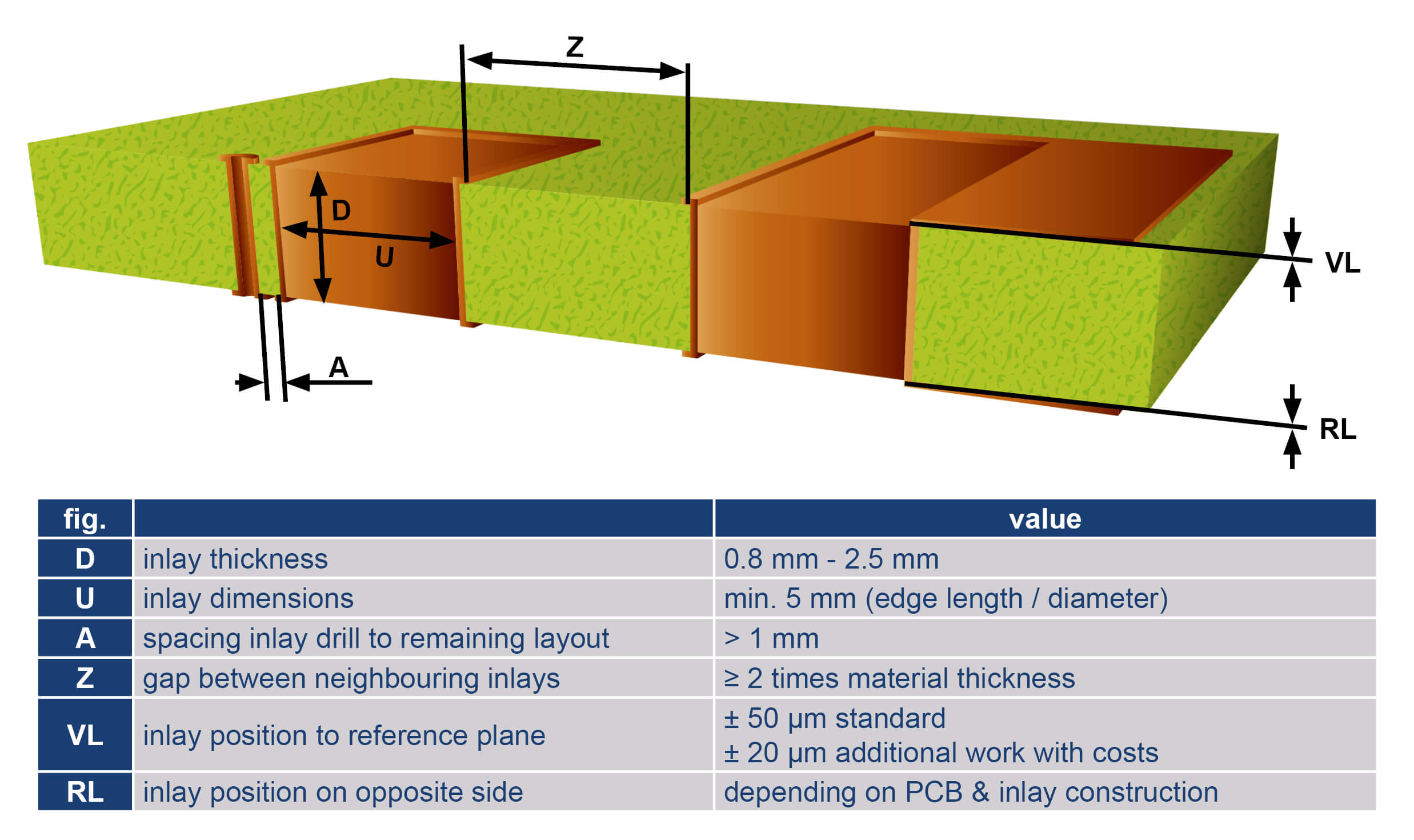
In Metal Inlay Technology a massive copper element (inlay) is pressed into the printed circuit board and serves to dissipate the heat of an electronic component through the printed circuit board. The heat-emitting component (heat source) can be connected directly to the metal inlay. Copper inlays with a minimum diameter of 5mm and a thickness of 0.8-2.5 mm are used primarily for this. Depending on their shape and dimensions, the metal inlays are inserted fully or semi-automatically.
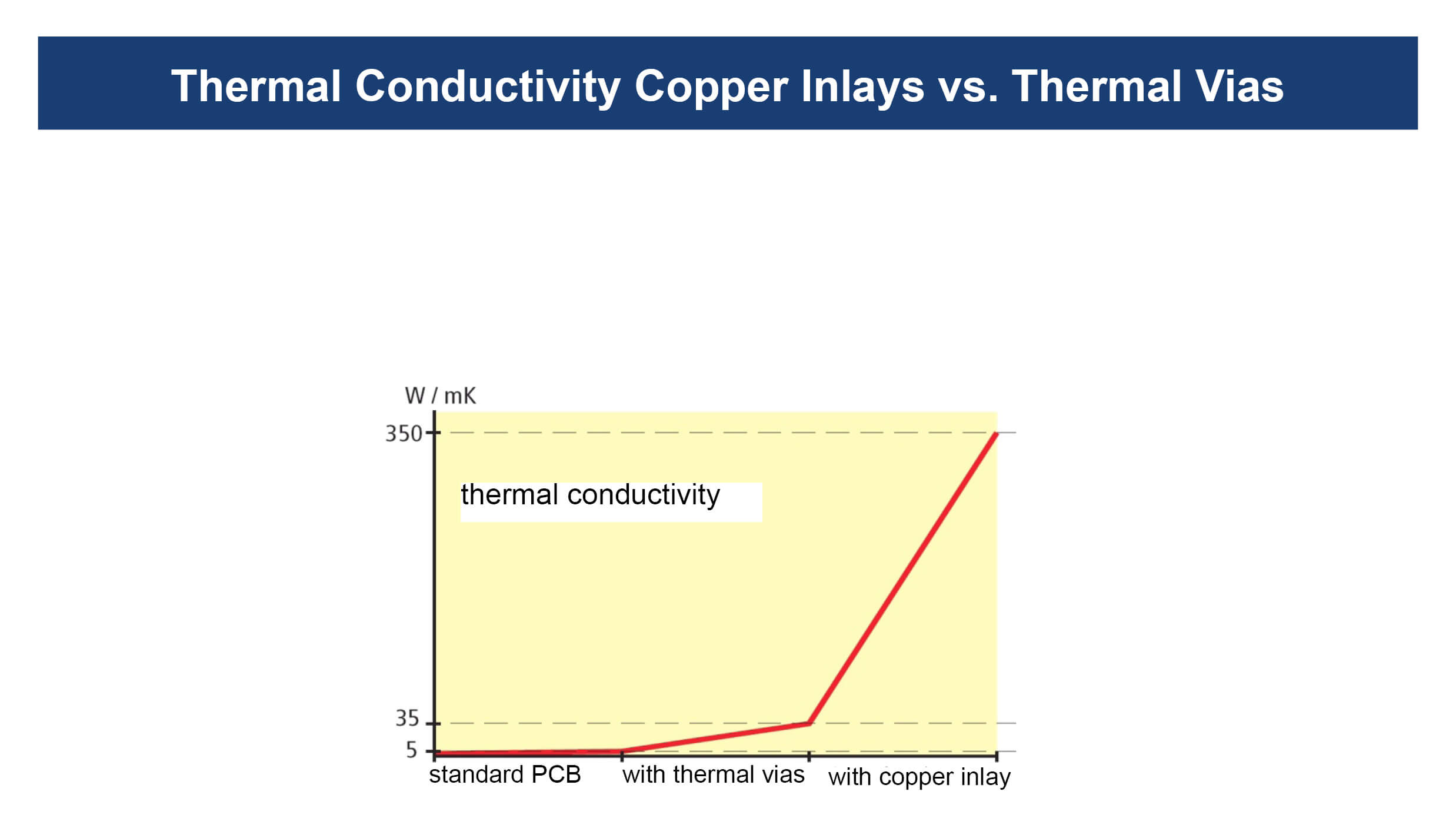
The use of metal inlays allows substantial improvement of the thermal conductivity (through the printed circuit board) compared with conventional thermal vias.
Any shape can be chosen for the metal inlays (square, round). The required recesses in the printed circuit board are produced by milling or drilling. Mounting holes up to a diameter of 6.35 mm can be produced during the first drilling procedure and are therefore cost-efficient.
Applications:
- E-Mobility & automotive: Motor controls (ECU), ABS, ESP, start-stop systems
- industrial electronics: inverter and rectifier, power electronics, control electronics
- lighting technology: LED lighting, special projectors and cinema technology
Advantages:
- optimal heat dissipation through direct connection of the component to the metal inlay (soldering, gluing etc.)
- optimal heat conduction through the printed circuit board: the continuous copper path enables excellent conduction from the heat source to the heatsink
- combination with other technologies possible, e.g. heatsink, semiflex etc.
- electrical connection of the metal inlays possible - also to the inner layers
- freedom to choose the geometry of the metal inlays
- fully automatic mounting of round metal inlays, semi-automatic mounting for other shapes
- very good planarity of the inlay to the reference layer (component or heatsink side)
Design Rules
Metal inlays can also be inserted in the inner layer core of a multilayer (e.g. sequential build-up). In this case they are called “embedded metal inlays“. The contact to the inlays is established here by lasered or mechanically drilled blind vias.
Reliability Tests:
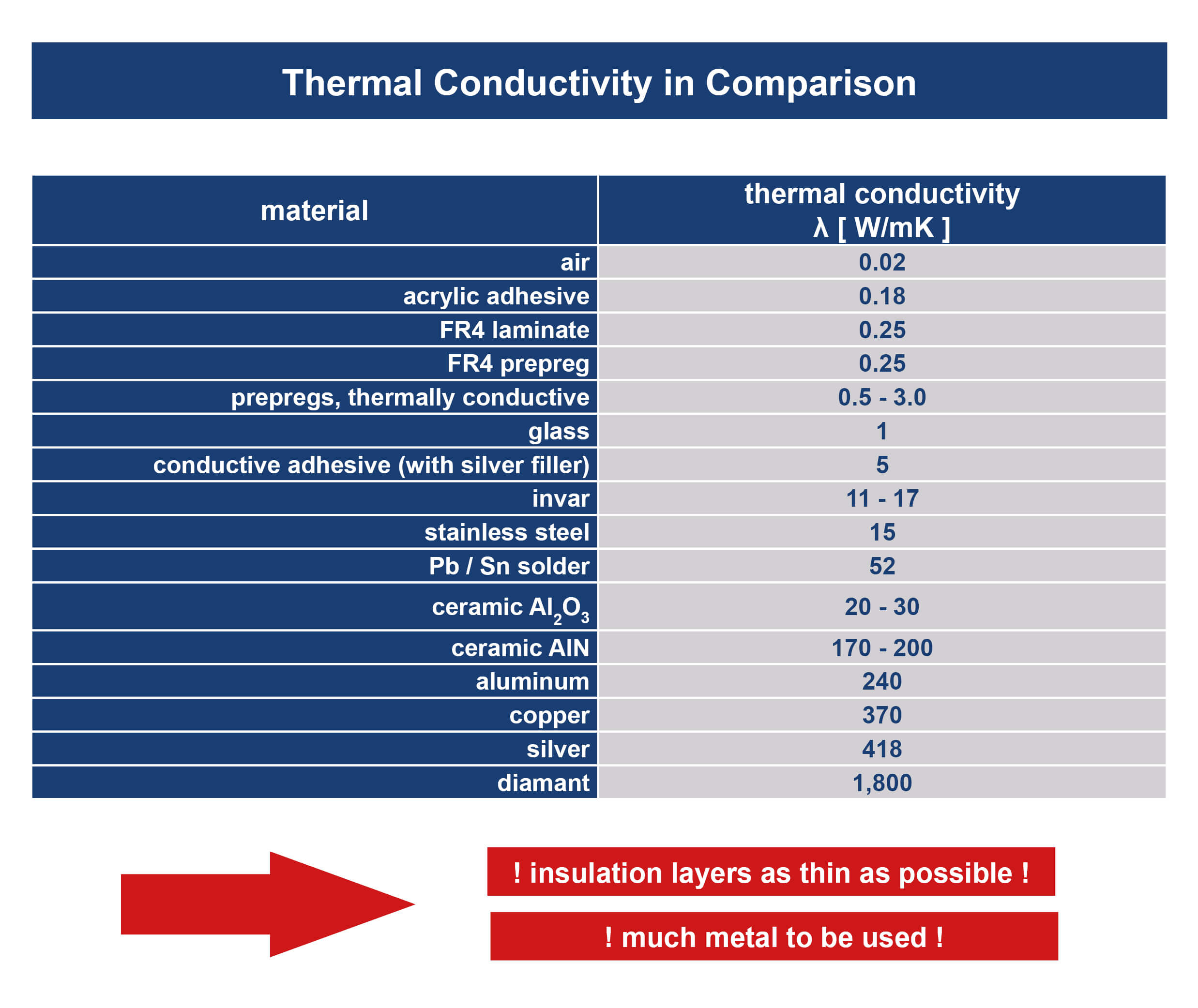
Compared to metals, electrical insulating materials are very bad thermal conductors.
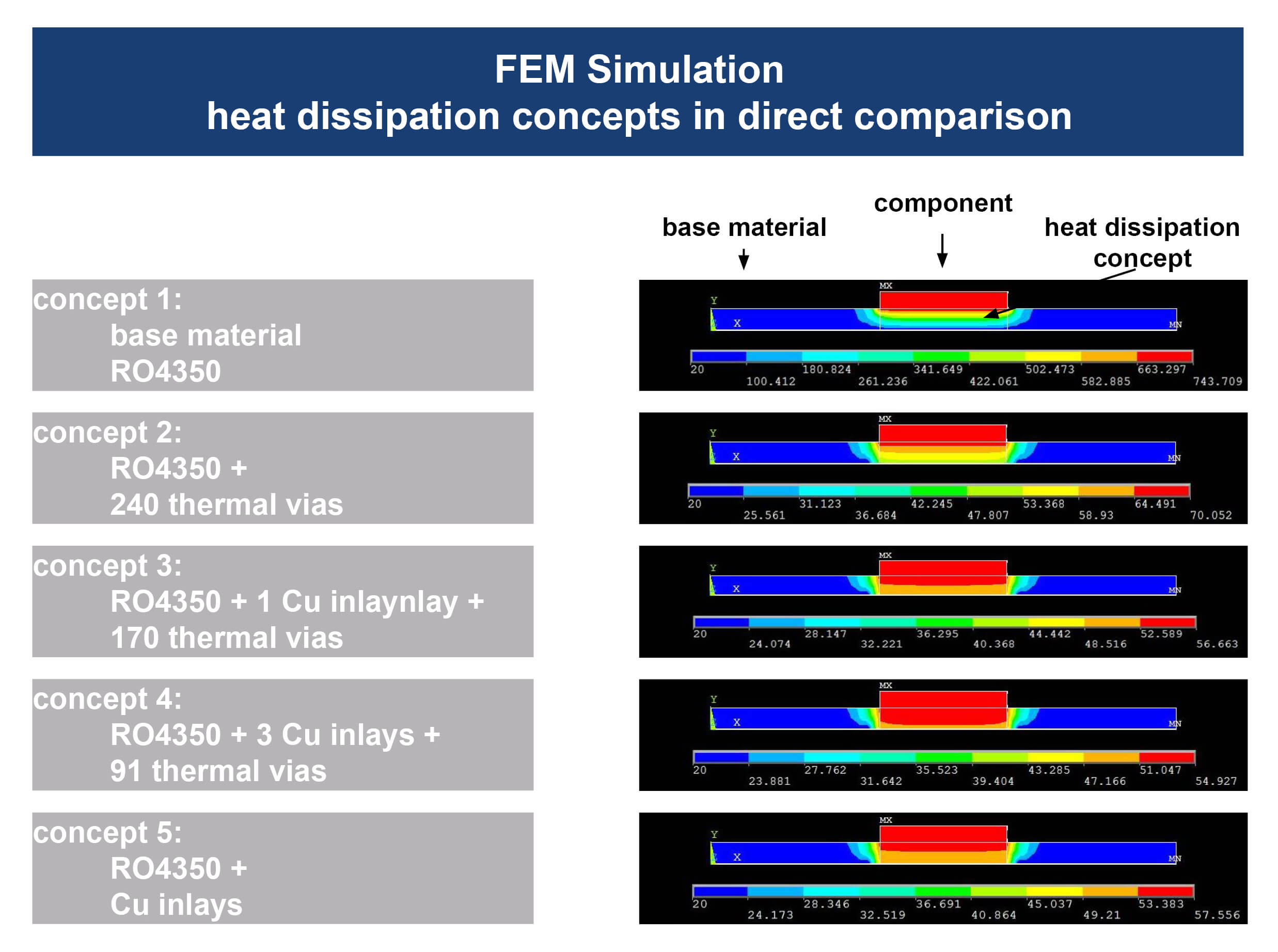
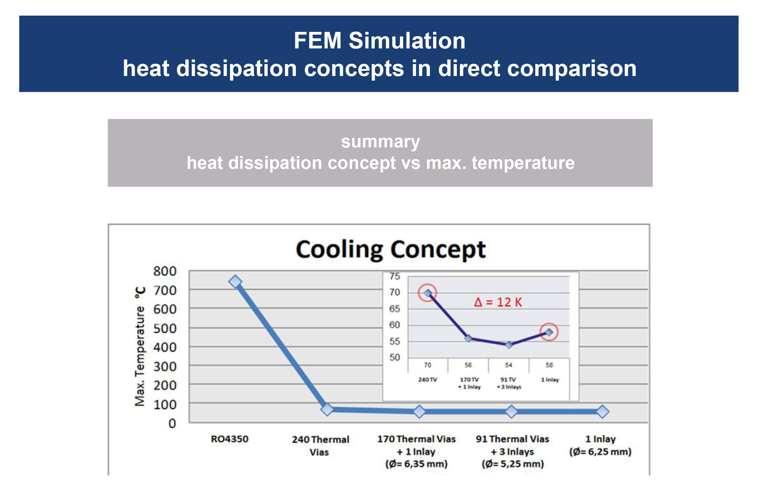
FEM Simulation - Heat Dissipation Concepts in Direct Comparison
Applications
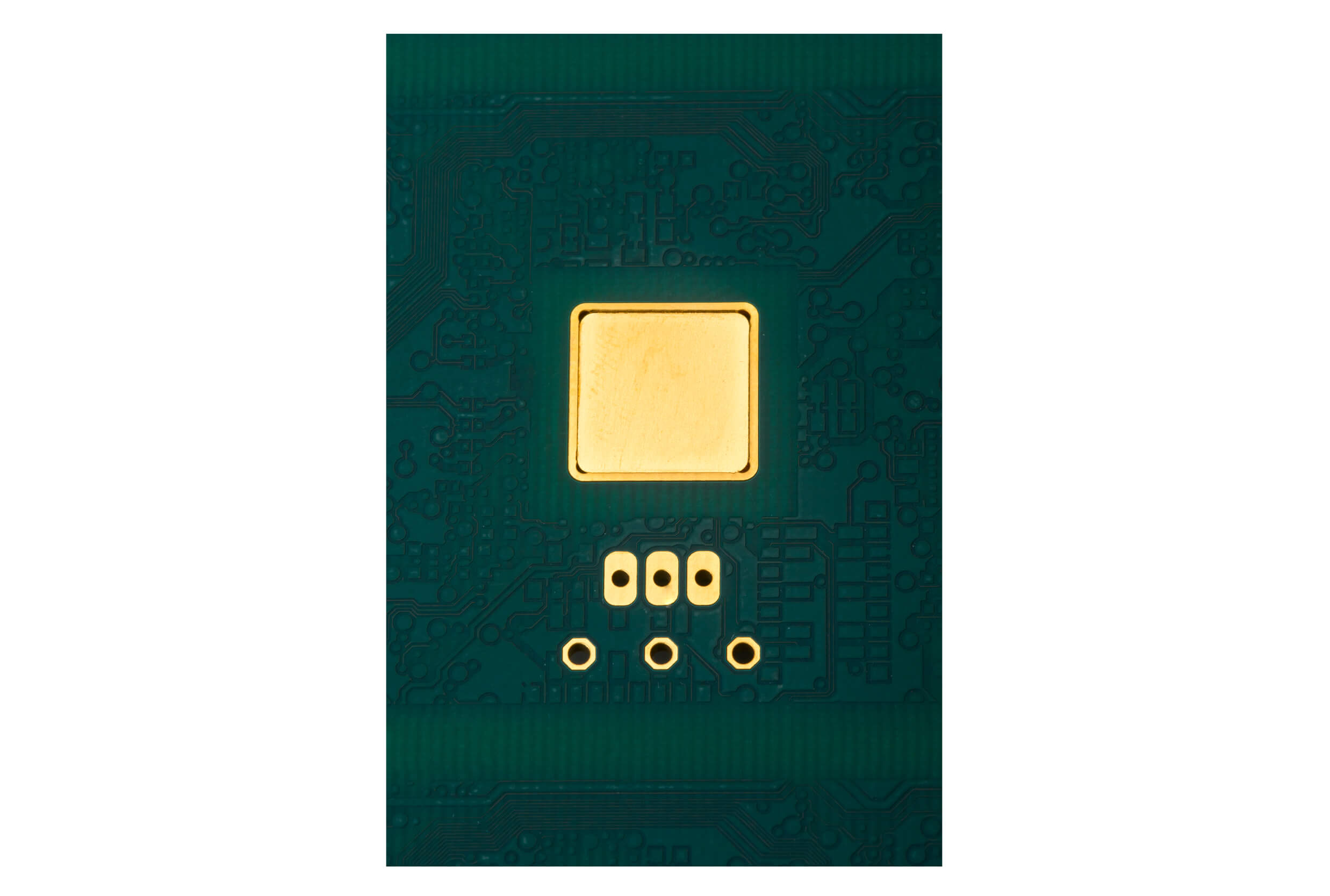
Inlay mounting
High power LED
Contact to product management:
product management
+49 (0) 2831 - 3 94-0
info@unimicron.de
Further PCB Technologies:
Thick Copper Technology - HiCu PCB | Thick Copper Profile Technology - HiCu Profile PCB | HDI Technology - HiDensity PCB | High Frequency Technology - HiFrequency PCB | IMS & Heatsink Technology - Metal Plate PCB | Semiflex Technology - Semiflex PCB | Partial Thick Copper Technology - Wirelaid®