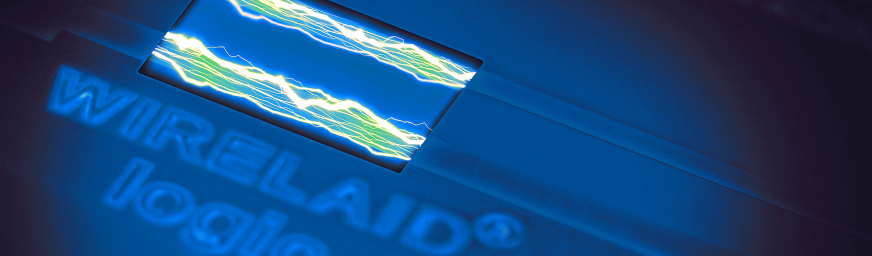
Partial Thick Copper Technology - Wirelaid®
An Alternative for Partial Currents up to 100 A
Wirelaid is a patented printed circuit board technology used by Unimicron as licensee. In Wirelaid Technology copper wires are applied to the treatment side of a copper foil (thickness 35-105 μm) by micro resistance welding. The wires used are round wires with a diameter of 300μm and flat wires with dimensions of 250 μm x 800 μm or 350 μm x 1400 μm in any length. During the manufacturing of multilayers these wires are embedded in the resin of the respective printed circuit board construction.
Wirelaid Technology can be an alternative and cost-efficient solution in cases where a high copper cross-section is only partially required within a printed circuit board. Here basic copper in standard thicknesses (35μm-105μm) can be used, reinforced in the specified areas by appropriate wires. By combining different wire geometries and varying the number of wires, the current load capacity can be increased while reducing conductor warming at the same time. The total copper component is lower than that in thick copper technology, which also has positive effects for instance on the soldering process.
In addition, a lower consumption of etchants and shorter etching times help to reduce costs.
Applications of Wirelaid®:
- heat dissipation in critical areas by partial increase of the copper cross-section
- combination of power and control electronics in or on a printed circuit board
- high current applications (up to 100A) where a higher wire cross-section is only partially required
- to a certain extent mountings can also be optimised by special V-scoring
Technical Features:
- wires are laid by a CNC-controlled machine
- surface is planar as the wires are laid inside the printed circuit board
- significant gain in surface space, the actual layout structure itself is scarcely affected
- enhanced heat dissipation at hot spots, similar to that of thick copper
- layer count in multilayer PCBs can be reduced
- reduction of copper thickness, costs reduction
- combination of power and control electronics on one layer
- many common printed circuit technologies can be combined with Wirelaid
Manufacturing Process:
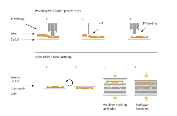
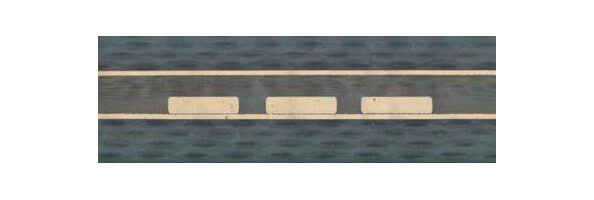
Microsection with embedded flat wires
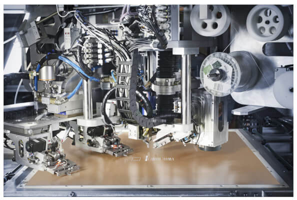
Compared with other processes, in Wirelaid Technology the wires are laid, welded and cut au- tomatically using cutting-edge CNC equipment.
The Position of the Wires:
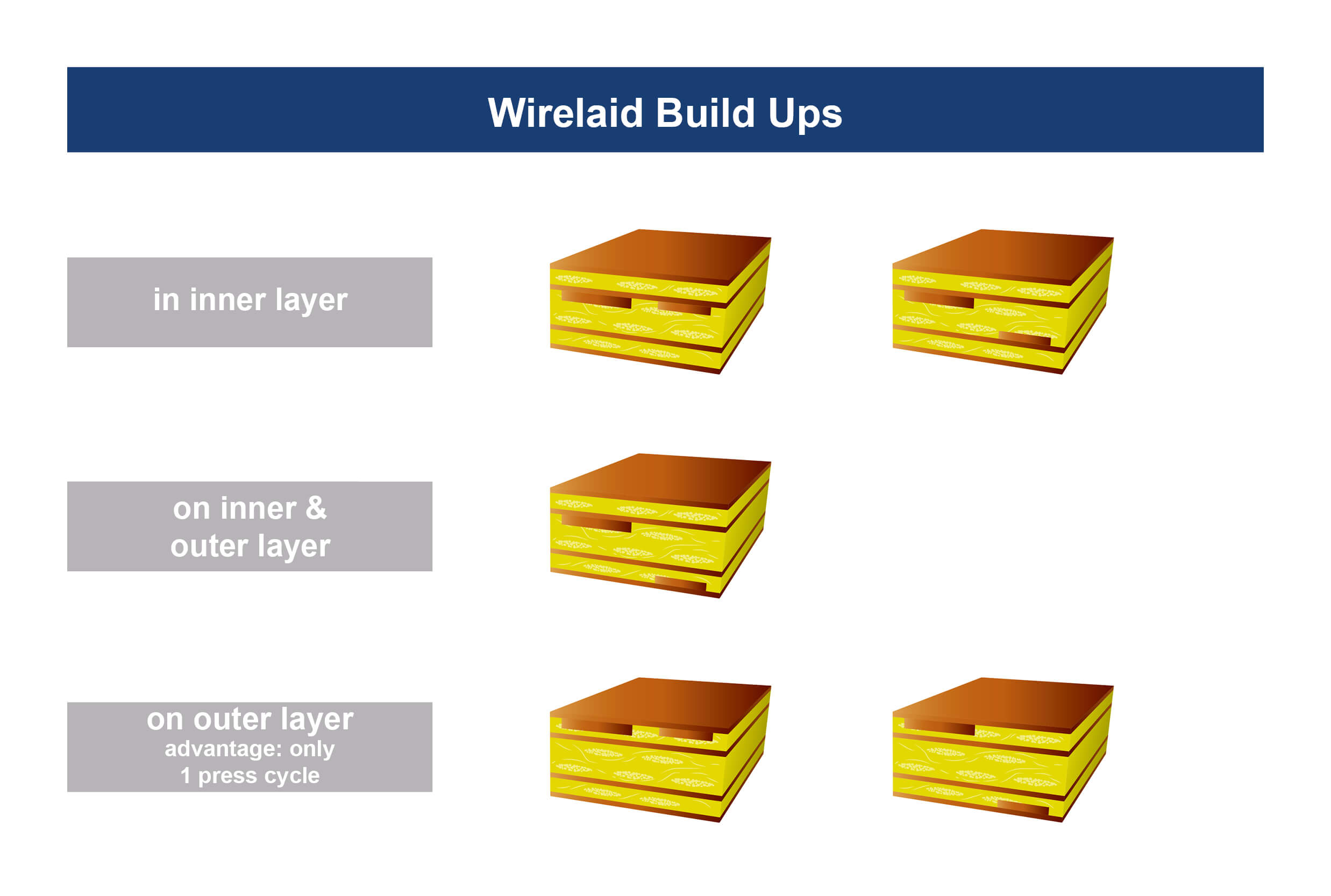
Detail of a layout with “reinforcement” by wires (green: wires / red: Cu layout)
Applications
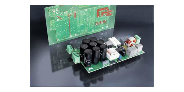
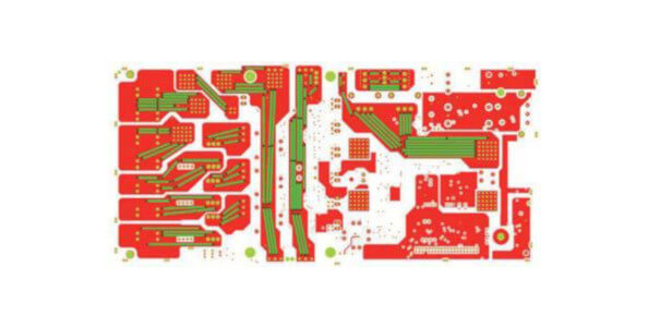
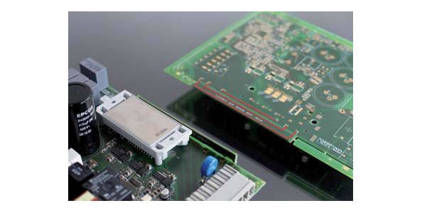
Power supply for servo drive control (partial 70 A on 105μm Cu foil & wires / red: position of the wires)
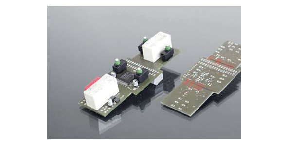
Switch unit (red: position of the wires)
Processor-controlled drive control (red: position of the wires)
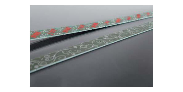
LED helical lamp (red: position of the wires)
Contact to product management:
product management
+49 (0) 2831 - 3 94-0
info@unimicron.de
Further PCB Technologies:
Thick Copper Technology - HiCu PCB | Thick Copper Profile Technology - HiCu Profile PCB | HDI Technology - HiDensity PCB | High Frequency Technology - HiFrequency PCB | Metal Inlay Technology - Metal Inlay PCB | IMS & Heatsink Technology - Metal Plate PCB | Semiflex Technology - Semiflex PCB