Preparatory Positions
Design for Manufacturing
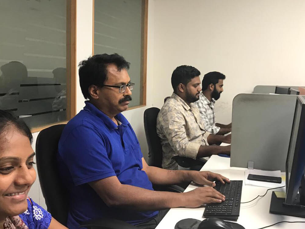
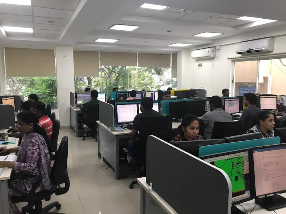
In addition to the commercial process, the technical preparation and checking of the data is one of the most important processes prior to manufacturing. Our sales team as well as part of our operations scheduling is located in Geldern. We have also installed our own offices with more than 25 specialists in India, where the majority of data preparation takes place.
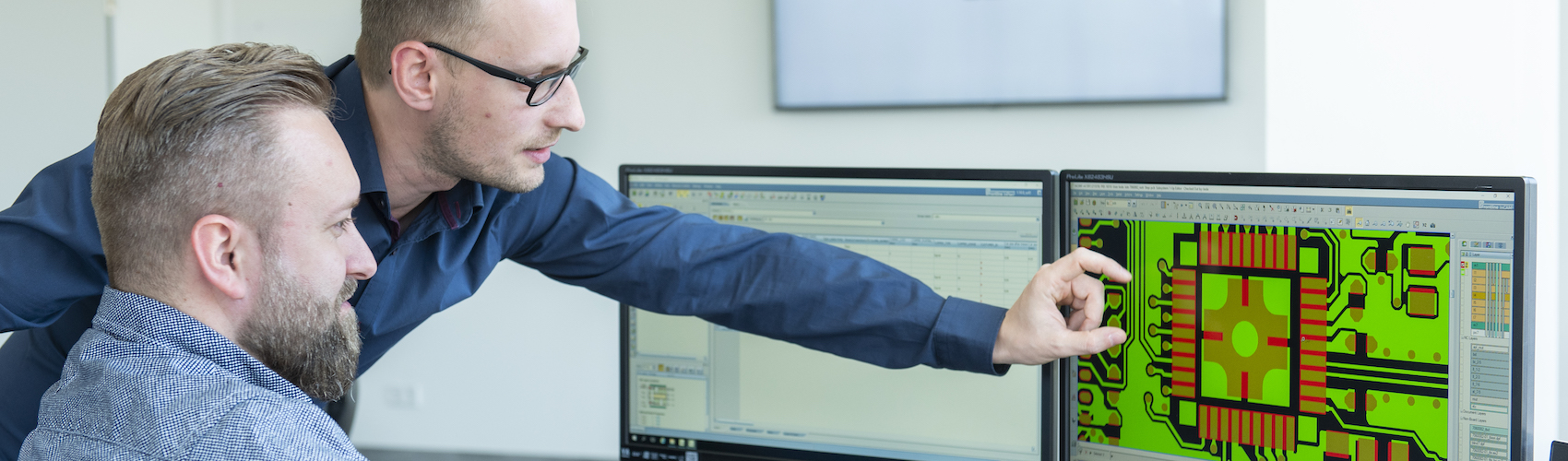
The customer data in the common Gerber format is entered by us and checked for feasibility. The Gerber data describes each individual layer of a PCB as well as the solder resist mask and any labelling or the position print.
In the so-called design rule check, we check, for example, residual rings, pitch spaces and the solder resist mask.
Our specialists collaborate closely with our customers. After approval, they place the single panel or assembly panel into the manufacturing panel and write the corresponding drilling and milling or notching programs as well as the programs for the exclusively digital exposure in the photo print inner and outer layers and solder resist mask and E-test via adapter and flying test.