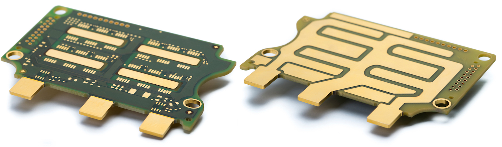
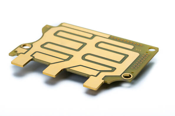
Thick Copper Profile Technology - HiCu Profile PCB
Embedded Copper Technology as an Alternative for Partial Currents up to 1,000 A
In HiCu Profile Technology massive copper elements are inserted in the inner cores of multilayer printed circuit boards and then laminated into the PCB. In this way the copper cross-section is partially increased - but only where the high current-carrying capacity (up to 1,000 A) is required.
This technology can often be an inexpensive alternative to conventional thick copper technology as regards current-carrying capacity and heat dissipation.
The copper profiles used are between 0.5 and 2.0 mm thick.
Applications:
- power electronics
- high current-carrying capacity up to 1,000 A
Advantages:
- excellent heat dissipation due to direct connection of the component to the copper profiles, e.g. possible through cavities and blind via-holes
- combination of fine structures with high currents on one printed circuit board possible
- combinable with other technologies like thick copper, HDI, semiflex
- weight saving and reduction of thickness possible
Manufacturing Process:
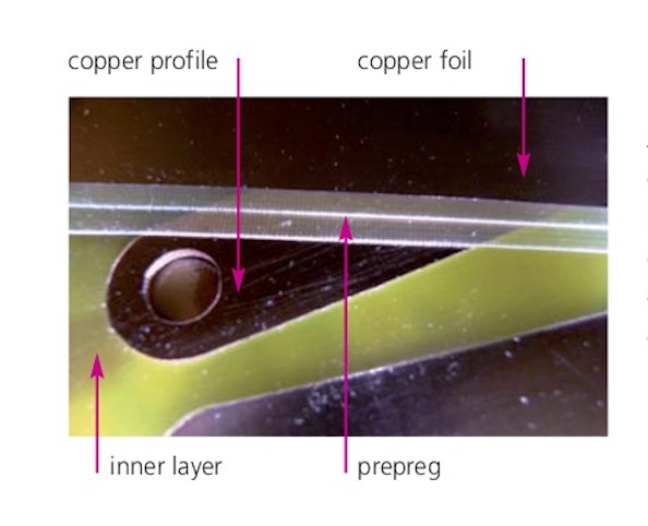
1. First the appropriate contour is established by milling or punching a recess in the inner layer core.
2. The copper profiles are then placed in the recess.
3. Then the prepregs and copper foils are laid up.
4. After lamination of the multilayer the usual process steps follow to finish the printed circuit board.
A great advantage of HiCu Profile PCB is the easy combination of control electronics (outer / inner layer) and power section in the inner layer core on one board. Even fine structures via HDI technology can be realised there.
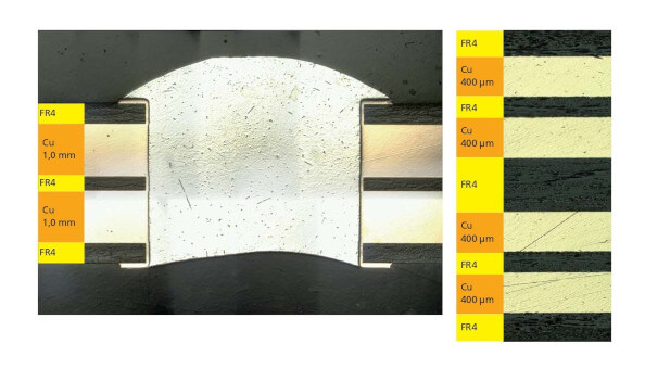
As shown in the above figures, even a number of inner layers can be equipped with copper profiles. HiCu Profile Technology can also provide an important cost advantage where it permits replacement of thick copper layers with a copper thickness of 210 μm or 400 μm. In this specific application four inner layers each with 400 μm copper could be replaced by two inserts of 1 mm each. This reduces the overall thickness of the printed circuit board by approx. 0.5 mm
Design Rules
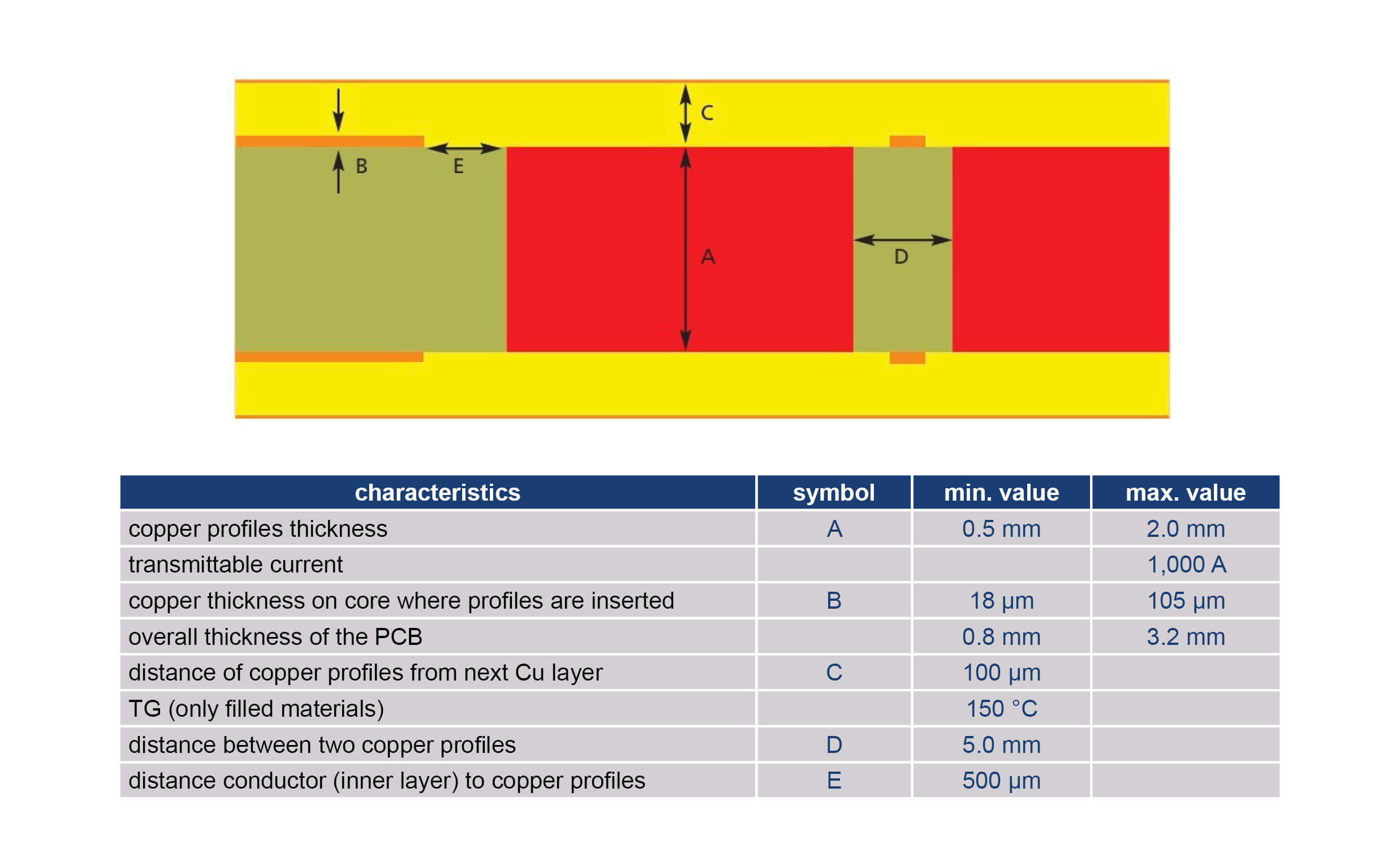
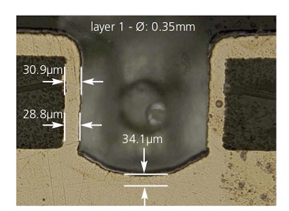
Copper profile connected by blind via to the outer layer.
Applications:
Contact to product management:
product management
+49 (0) 2831 - 3 94-0
info@unimicron.de
Further PCB Technologies:
Thick Copper Technology - HiCu PCB | HDI Technology - HiDensity PCB | High Frequency Technology - HiFrequency PCB | Metal Inlay Technology - Metal Inlay PCB | IMS & Heatsink Technology - Metal Plate PCB | Semiflex Technology - Semiflex PCB | Partial Thick Copper Technology - Wirelaid®