Plating Through and Photo Print
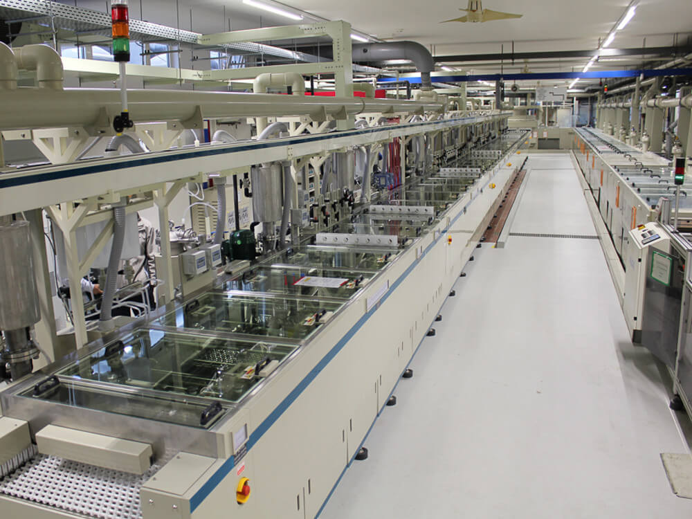
Plating through is used for the electrical connection between the individual copper layers on a PCB. Using a chemical copper deposition, the bore holes’ hole walls are provided with copper after drilling.
For photo printing, the conductive pattern is applied to the outer layer. This is done using absolutely state-of-the-art direct exposure via laser on a photo-sensitive foil which is previously attached. Compared with exposure with films which used to be applied, this process is considerably more precise and efficient. Then, the pitch spaces of 0,3 mm can be realized, meeting the requirements regarding miniaturization.